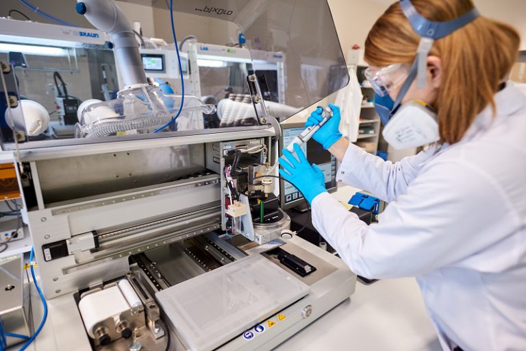
Organic electronics Organic electronics High resolution contact measurement of the surface profile with the roughness analysisMapping the shape of the mask on the substrate – performing the first and subsequent levels of photolithographyOptimization of production processes of active layers using solution methods: – in glove boxes system – in CLEANROOM ISO5Full characterization of optical and electrical properties of organic thin layersProduction of optoelectronic devices with vacuum and/or solution methods with full electrical characterization and encapsulationSurface activation/surface cleaning using the active plasmaDetermination of liquid or thin layer absorbanceOptimization of process of applying paths using ink based on a tested material with conductive propertiesOptimization of the physical vapor deposition process of organic compoundsOptimization of the physical vapor deposition process of the metallic layer (e.g. Ag, Au, Al, Ca, etc.)Determination of electron affinity in moleculesExamining of the HOMO / LUMO levelsStudies on polarization of particlesInfluence of substituents on the charge transfer properties Contactdr Sylwia Kotarba+48 42 280 76 84+48 515 669 719 Contact form Email address (required) Subject Message I agree to let process my personal data in order to send me answer to enquiry in accordance with the Personal Data Protection Act of May 10, 2018 and the EU Genareal Data Protection Regulation 2016/679( Regulation (EU) 2016/679 of the European Parliament and of the Council of 27 April 2016). Disclosing the personal data is voluntary. I have been informed that I have the right of acess to my data, its rectification and erasure. Bionanopark sp. z o.o. is the controller of my personal data.